Discussion
For my popcorn 1.5 watt CW transmitters, I normally use a variant of the Ugly Weekender Transmitter designed by Wes Hayward, W7ZOI. This transmitter is quite similar to the design used by Roy Lewellan, W7EL in his Optimized QRP Transceiver article in 1980.
Presented are several transmitter topics; the Chickadee crystal-controlled novelty transmitter, the Ugly Weekender revisited, a QRO HEXFET power amp for 80 meter band CW and a 6M crystal controlled CW transmitter.
Last updated Sept 6, 1999.
Chickadee Transmitter
![]()
Chickadee Notes
The Chickadee is a 40 Meter transmitter and crystal Y1 is a 7.0400
MHz, AT-cut in a HC-6/U metal holder with 30 pF load capacitance. No feedback
capacitor(s) were needed across the crystal in the Pierce oscillator as
oscillation started every time the key was pressed without them.
The
original Chickadee circuit resembles a simple tube transmitter and as shown with
a VCC of 13.8 VDC has an output power of 35 - 40 milliwatts. If the VCC is
increased to 22 volts or so the output power may increase to 50 - 60 mW. Jeff
Damm, WA7MLH suggests AC bypassing the source resistors to ground with 0.01 or
0.1 uF capacitors to get more output power out of the original schematic. More
power maybe also achieved by using hotter JFETs such as the J310.
Keying this
little transmitter, grounds the source resistors of both Q1 and Q2 and results
in very clean transmission with no backwave problems. Admittedly, the keying
sounds a little hard, however for a low parts count rig, it is
acceptable.
The Q1 1 mH and Q3 22 uH RF chokes are simple epoxy units
which resemble resistors. The T1 transformer is wound with 37 primary and 8
secondary turns over the cold end of the primary coil wound on a T50-2 core. XL
= 300 ohms and the capacitance needed to resonate this transformer is
approximately 76 pF which is easily done with the paralleled 68 pF and 20 pF
trimmer caps shown in the schematic.
The original 2 stage Chickadee had no
low pass output filter.
Adding the Q3 stage boosts the output power to
over 370 mW at a VCC of 13.8 volts. Like the Q2 nJFET stage, Q3 is a simple
Class C amplifier. The choice of transistors for Q3 is numerous, however a
press-on heat sink is required to protect Q3 from heat damage. The output pi
filter as shown is from Doug DeMaw, W1FB and provides both low pass filtering
and a 50 ohm impedance transformation. The 3.48 uH inductor can be wound using
27 turns on a T50-2 core using #24 AWG wire. This project is shown chiefly for
reference and sentimental reasons and provided much fun on 40 Meters and was
used extensively for local code practice in its original 2 stage
form.
The Ugly Weekender Revisited
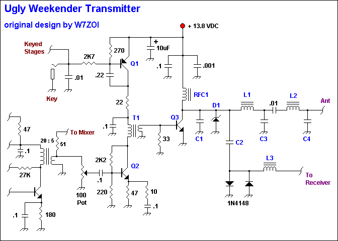
Ugly Weekender Transmitter Revisited Notes
The original project is from The
Ugly Weekender: parts 1 and 2 , by Roger Hayward, KA7EXM and Wes Hayward, W7ZOI,
QST for Aug 1981 and June 1992. The Ugly Weekender articles are mandatory
reading for any homebrew radio enthusiast. I have built this transmitter section
for 4 different amateur bands ( 160, 80, 40, 30 ) and it has never failed to
function perfectly.
Presented will be the necessary data to put this
transmitter section on any band that you chose.Ugly It Is
Schematic Explanation
The schematic above
depicts the transmitter section connected to a partial schematic of the VFO
buffer/amplifier stage. This VFO design is used in for the Popcorn Superhet
projects on this web site.
The keying switch from the original design has
been removed from the VFO circuitry and placed in the transmitter section. It
maybe preferable to place the transmitter keying switch with the transmitter
stages as shown and keep the VFO transmit offset circuit in the shielded VFO
box. The keying switch consists of the parts connected to and including Q1. Q1
is a 2N3906, however any general purpose PNP transistor will work as well. The
keyed waveform has a smooth rise and fall shape and is clickless.
Q2 can
be a 2N3094 or any related NPN transistor such as the 2N2222 or 2N4401. The only
major difference from the original schematic on the Q2 stage is the T2
transformer. The original article used two broadband 4:1 transmission line
transformers to drive the Q3 stage with a low input impedance. This schematic
uses one conventional broadband transformer to achieve the same purpose. This
transformer T1, is wound on a FT37-43 ferrite toroid using 12 primary turns and
3 secondary turns distributed evenly over the primary windings. Use number 26
AWG enamel-covered wire. Balun cores such as the BN73-201 are also suitable,
although be sure to preserve the 16:1 impedance transformation ratio.
The
Q3 stage RF choke RFC1 can be wound using 10 - 12 turns of number 24 AWG enamel
covered wire on an FT37-43 ferrite core or as indicated in the original article.
The Q3 transistor choices include the 2N3866 or 2N3553 or similar BJT with a
heat sink. QSK and Low Pass Filter Sections
Low
Pass Filter
The low pass filtering in this transmitter is
achieved by connecting two 50 ohm PI filter sections together with a 0.01 uF
coupling capacitor. While these sections could be connected together in a
tradional half-wave filter fashion and the coupling cap placed before the
filter, the method used by W7ZOI leads to easy filter design. The first order of
business is to determine what cutoff frequency to use. One easy way to determine
the -3dB cutoff frequency is to build a filter around standard value capacitors
since you can always wind any needed inductances on powdered iron toroids. The
Pi-Filter program offered on this web site makes this exceedingly easy and saves
a lot of number crunching. You can chose the cutoff frequency to suit capacitors
that you have on hand or by trying to get close to a desired cutoff frequency
using standard value capacitors.
The following text refers to the below Pi
Filter schematic for clarity however the principles are easily applied to the
Ugly Weekender transmitter filter stages:

Consider the original low pass filter for 40 meters. Wes
Hayward chose a cutoff frequency of 7.40 MHz which means that the individual Pi
filter elements are 1.08 uH for the inductor ( L1 ) and 430 pF for each
capacitor ( C1 and C2 ). I placed a 100 pF cap in parallel with a 330 pF cap to
get the 430 pF capacitance in my version of the 40 meter low pass filter. He
could of easily chose a 390 pF capacitor on each side of the filter for a cutoff
frequency of 8.18 MHz. How close to the band edge frequency you want to get is
up to you. If you want to have an fco just above the higher band limit you will
probably have to parallel 2 capacitor values as W7ZOI did. If you are a more
frugal builder, you can use the nearest standard value capacitor that will
provide an fco above your upper band limit. Using software to determine the
filter elements is the most rapid method to do this, but here are the formulas
right out of the PI Filter program:
Cutoff Frequency = 1000000.0 / (
Capacitance * 6.283 * 50.0)
The Frequency answer will be in MHz and
the Capacitance variable refers to the picofarad value for C1 and C2 which are
always the same value ( C1 = C2 ). If you parallel 2 caps for C1 and C2, use the
total capacitance value for the Capacitance variable.
Inductance =
50.0 / ( 6.283 * Frequency )
Inductance answer will be in
microhenries and the Frequency variable is in MHz.
Lets build a filter
for the 30 meter band. The largest standard value that you can use for C1 and C2
is 270 pF, which gives a cutoff frequency of 11.79 MHz. This maybe acceptable to
you however perhaps you would like a cutoff closer to the upper band limit of 30
meters. Placing a 33 pF cap in parallel with C1 and C2 would result in a total
capacitance of 303 pF and an fco of 10.51 MHz. This would be a great filter. The
required inductance to resonate 303 pF at 10.51 MHz is 0.76 uH. Using the
CoilBulder program this can be constructed with 14 turns of number 22 AWG enamel
covered wire on a T50-6 core.
The above formulas can be used to build filters
using standard capacitor values for C1 and C2. The only problem is that you need
to start with a capacitance value and substitute the value up or down with
standard or paralleled cap values to reach the desired cutoff value. The
starting capacitance can be determined with a formula:
Capacitance =
1000000.0 / ( 6.283 * Cutoff Frequency * 50.0 )
Capacitance answer is
in pF. Cutoff Frequency is in MHz and is the desired cutoff frequency for your
filter.
The starting capacitance formula will get you going and you can
use either the program or other formulas to design your filter. Another
alternative is variable capacitors and/or inductors, but I will not go
there.
Once your filter is designed, all that is left is to design the values
for series-resonant T/R components C2 and L3 of the Ugly Weekender Transmitter
schematic on this web page.
Transmit / Receive
Circuit
The following text now refers to the Ugly Weekender
transmitter schematic on this web page.
The Ugly Weekender transmitter
featured a clever circuit to provide QSK switching when used as part of a
transceiver. The antenna is connected to both the receive input and the
transmitter output at all times. While transmitting, the back-to-back diodes in
the schematic conduct and prevent the RF level from exceeding 0.7 volts RMS. I
have used this scheme with power output levels of over 50 watts using a higher
inductance to capacitance ratio to keep the current in the diodes low. The W7ZOI
T/R scheme also adds selectivity for the receiver as the antenna input is
connected to the receiver through a low pass filter. It is necessary to design a
series-resonant circuit to connect the low pass filter to the receiver in order
to minimize signal loss on receive. The inductive reactance of the inductor L3
and the capacitive reactance of capacitor C2 are equal at the operating
frequency. It seems that using a reactance of ~450 ohms at the lower band edge
works well.
To design this circuit, first get the value for C2 by the
following formula :
Capacitance = 1000000.0 / ( 6.283 * Lower
Band-Edge Frequency * 450.0 )
The Capacitance answer will be in pf
and the Lower Band-Edge Frequency is in MHz.
For the 40 meter band this
means that C2 is 51 pF. If I only had a 47 ohm capacitor on hand, I could
substitute a 47 pF value for C2. This of course means that my XC is no longer
450 ohms and I will need to re-calculate the capacitive reactance as the XC
value is also the inductive reactance value ( XC = XL at resonance ) which is
needed to calculate the inductor value for L3.
Capacitive Reactance =
1000000.0 / ( 6.283 * Capacitor Value * Lower Band-Edge Frequency )
Capacitive reactance is in ohms, Capacitor Value in pF and Frequency
in MHz.
You will need to do this whenever the 450 ohms capacitive
reactance value does not not give a standard value capacitor. Simply substitute
the nearest standard value or parallel an additional capacitor to get near the
value and re-calculate the XC. Use the XC and thus XL value to calculate the
needed inductance for inductor L3 using this formula :
Inductance = XL
/ ( 6.283 * Lower Band-Edge Frequency )
If I used the 47 pF cap for
C2, the XC = 484 ohms and the required inductance for L3 = 10.2 uH. In Wes
Haywards original article a 51 pF cap was used for C2 and L3 was 10.1 uH and the
XC/XL = 446 ohms.
The final variable to be calculated is the new
capacitance for C1. When transmitting, C1 and C2 are effectively in parallel and
the C2 value must be subtracted from the original Pi filter C1 value. As you
recall, the value determined for C1 when doing the PI Filter calculations was
430 pF in Wes Haywards design for 40 meters. Subtracting C2 from C1 = 430 pF -
51 pF = 379 pF. Wes used a 390 pF value for C1, substituting the nearest
standard value capacitor.
Lets calculate all the values for a 15 meter
band output section using standard value capacitors :
Cutoff Frequency chosen
= 21.65 MHz. C1 = 120 pF, C2 = 18 pF, C3 = 147 pF, C4 = 147 pF, L1 = 0.37 uH, L2
= 0.37 uH and L3 = 3.19 uH.
Ideally C1 should have been C3 - C2 or 129 pF ,
however a 120 pF value was substituted. I believe that it is better to go low
with the C1 value as the Zener diode D1 exhibits some capacitance to the circuit
as well. For C3 and C4, parallel a 120 pF with a 27 pF capacitor to make the
required 147 pF. The inductors are easily wound on powdered iron
toroids.
Series-Resonant Variations
A
slightly different variation of the series resonant circuit works well on 80 and
40 meters. A RFC of 15 uH is used as the inductor for L3. At 3.5 MHz, this choke
has an inductive reactance of ~330 ohms. The capacitance to resonate the circuit
( C2 ) is ~138 pF. Since your choke is generally off by 10% or more it is
necessary to tune the C2 value by placing a fixed value cap in parallel with a
trimmer cap so that the circuit can be peaked for maximum signal strength to the
receiver. The choke value is not critical as Qu is low and bandwidth is high,
but tuning is necessary. For a transmitter on 3.5 MHz, I once used a 15 uH RFC
for L3 with a 68 PF cap in parallel with a 90 pF trimmer cap for the C2 caps and
this combination tuned perfectly. This circuit does not appear to critical with
respect to choke selection and the XL and XC values. Experimentation is fun and
can be used to suit the parts that you have on hand. Conclusions
An extensive body of work regarding QRP transmitters has been
written by the late Doug DeMaw, W1FB. His QRP NoteBooks and many articles for
QST and CQ magazines can provide a wealth of information to aid in the design
and building of QRP transmitters. Consult the web page entitled Selected QRP
Reading List for more information.
A 3.5 MHz HEXFET RF Power Amplifier
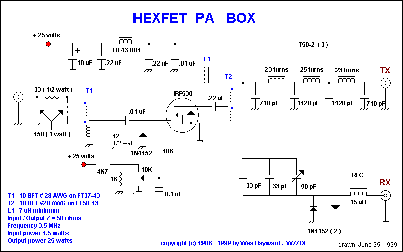
3.5 MHz PA Box For CW
Although , I am a tried and true QRP operator, it is nice
to run QRO at times when the band conditions are poor on 80 and 160 meters. A
few years ago, I asked Wes Hayward about using a HEXFET to make a brick for 80
meters and he gave me the above schematic. I built the project and it worked
very well. I worked many stations on the east coast and even worked an Italian
station using a folded Marconi antenna in the mountains while on a camping trip.
Unfortunately, while on the camping trip, the rig was run over by the truck and
camper and had to be given a decent burial.
This brick was excited with a VFO
controlled version of the Ugly Weekender which had an output power of 1.5 watts.
I could hook up the brick and run QRO or just use the QRP transmitter to suit
the band and battery conditions at the time. We generally placed two deep cycle
marine batteries in series to run this amplifier when camping.
Wes
Hayward published an article as QST Technical Correspondence in November 1989,
pages 38 - 40. This article should be in the library of anyone choosing to use
HEXFETS as a transmitter PA. The T/R scheme is described above in the
Transmit/Receive Circuit notes. Many thanks to Wes Hayward, W7ZOI for allowing
me to display this schematic.
A Six Meter Band Transmitter by VE7GC


VE7GC 50 MHz Transmitter for CW